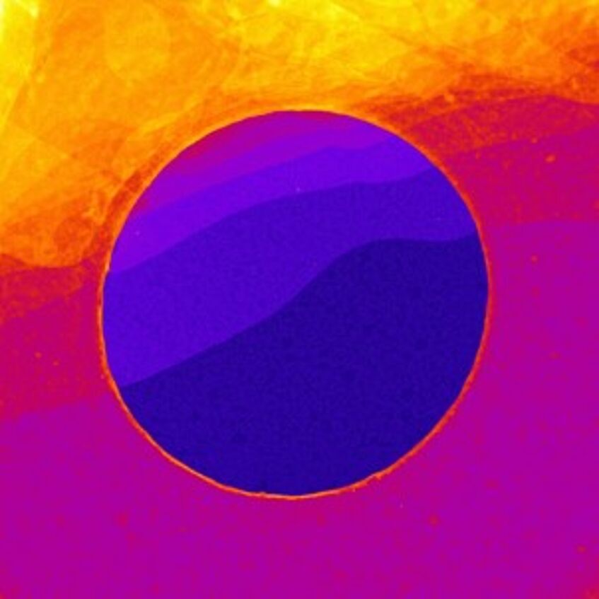
MoS2 on TEM grid irradiated by Xe
MoS2 on TEM grid irradiated by Xe
Title of the project: Electron-beam-induced chemical changes in 2d materials
Name of the VDSP student(s) & image credits: Umair Javed
Project supervised by: Jani Kotakoski
About me/us: I am PhD student in Physics of Nanostructured Materials (PNM). I'm working on electron microscopy of 2d materials.
Image: This is an image captured by MAADF (mid angle annular dark field) detector in Nion UltraSTEM 100 at Sternwarte lab. It depicts free standing MoS2 over the quantifoil hole. In dark field electron microscopy the heavier the particle is, the brighter the contrast is on the image. This is a particular spot of the sample is interesting. It shows a monolayer of MoS2 at the lower half of hole, then number of layers start increasing to a bilayer, then a trilayer and goes to 7-8 layers until we cannot distinguish among the layers, looks as if someone painted a landscape. In monolayers we see the pores created by Xe ions. The pores are harder to find when the number of layers increase. In this study we measure the impact of highly charged ions on 2d materials, it is a collaboration with University of Duisburg-Essen, Germany.

