Exploring Excellence in Electronics Manufacturing: A Day at AT&S in Leoben
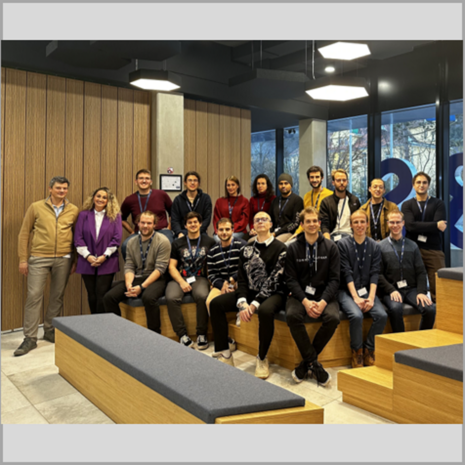
In an insightful career excursion to AT&S in Leoben, a global leader in the production of printed circuit boards, participants from our doctoral school delved into the heart of cutting-edge electronics manufacturing. The day unfolded as a journey of exploration, offering insights into AT&S's operations and providing a glimpse into the exciting world of printed circuit boards (PCB) and integrated circuit (IC) substrates. As we stepped into AT&S, participants gained a firsthand look into the company's operations. The AT&S-team led us through a comprehensive introduction, shedding light on the company's global reach and the intricate processes involved in the production, design, and optimization of PCBs and ICs. A highlight of the day was the engaging line tour, where participants witnessed firsthand the most pivotal steps in manufacturing. From etching and laser drilling to galvanic copper plating and rigorous quality control, every stage of the process was unveiled, providing a holistic understanding of AT&S's advanced manufacturing capabilities. As the excursion reached its end, participants seized the opportunity to discuss their prospects and explore potential applications of their skills within the AT&S environment.
We hope this excursion has proven insightful to all participants, offering not only a firsthand understanding of large-scale PCB and IC manufacturing, but also sparking curiosity and exploration into new possibilities for their professional journeys ahead.
By Viktor Birschitzky